// PCBEDITOR AI · SYSTEM CARD
Can you trust an AI-designed PCB? What to check before you order
An AI tool can hand you a placed and routed board in minutes. The useful question isn't whether it looks right. It's which parts of it were decided by a language model and which were computed, because those two kinds of output fail in different ways and need different checks.
This is the system card for PCBEditor, which turns a plain-English description into a placed, routed, design-rule-checked PCB with standard fabrication files. It explains how the work is split between the model and the deterministic engines, what that means for what you should check, and ends with a checklist to run before you send a board to a fab. PCBEditor is a hosted application, so no model weights come with this card.
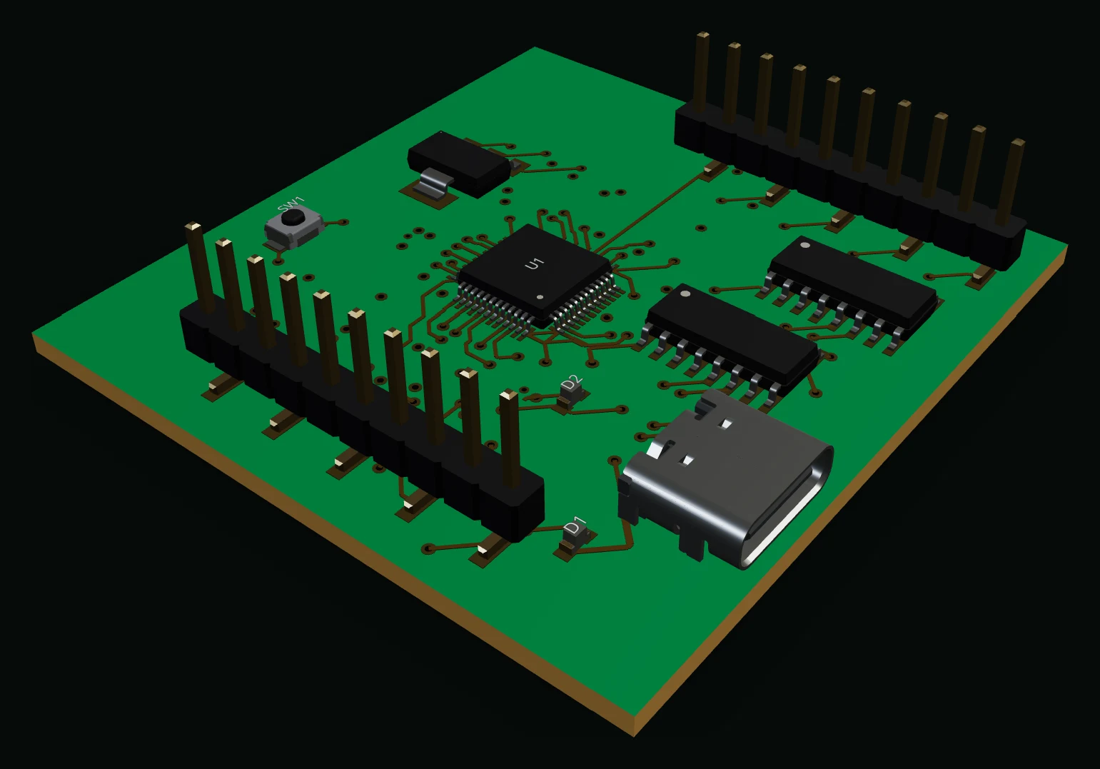 The 3D view: the board as an assembly, with the parts' 3D models in place.
Open PCBEditor →How the routing works
1. Know which decisions came from the language model
PCBEditor splits the job in two:
- Judgement, by a language model: choosing parts, proposing a topology, drafting the netlist. This is reasoning over prior art, which is what language models are good at. The system is model-agnostic and runs on hosted APIs (currently AWS Bedrock); no model is fine-tuned.
- Measurement, by deterministic engines: placement, multi-layer routing, design-rule checks and export. A language model has no way to measure whether a trace clears a pad by 0.15 mm, so it is never asked to. Routing is done by Sadie, an autorouter written in Rust (multi-layer A*, rip-up and reroute, Hammerstad–Jensen impedance modelling, graph-based connectivity proof).
What this means for your review: put your attention on the model's decisions, the parts and the connections. Mistakes there look plausible on screen: a wrong pinout or a missing pull-up resistor passes every geometric check. The geometry is computed, so check it with tools rather than by eye.
2. Expect the same board twice, but only from the same netlist
The model stage can return a different draft on a different run, and certainly on a different model version. The layout stage doesn't: the same netlist and the same rules give the same board. A review you did yesterday still describes the board you have today, even if the model behind stage one has been updated.
What this means for your review: once you have checked a schematic, keep it and build from it. Generating again from the same prompt gives you a new draft, and a new draft needs a new review.
3. Verify the board outside the tool that made it
The output is standard fabrication data: Gerber (RS-274X), Excellon drill, pick-and-place and BOM, plus a native KiCad .kicad_pcb file. That means you can check it with software you already trust:
- Open the
.kicad_pcbfile in KiCad and run its design-rule check with your fab's rules. - Load the Gerbers and drill file into a Gerber viewer and look at every layer, the board outline and the holes.
A result you can only verify inside the vendor's own tool isn't verified.
 The routing view: copper on each layer in its own colour, with vias and pads.
4. Read the unrouted list, not a percentage
When a board can't be fully routed, PCBEditor names the specific nets it couldn't complete instead of reporting a completion percentage. A figure like "94% routed" hides which connections are missing; a list of net names tells you exactly where to look.
What to do with it: most unroutable boards are placement problems. Move the parts at the ends of the named nets, give dense parts more room around them, and route again.
5. Know where it is weakest, and plan around it
- Dense fine-pitch BGAs are the hardest case. They need escape routing before a general router can help, and this is where you are most likely to see unrouted nets today. Plan for more layers or via-in-pad on those parts.
- It is not a signal-integrity suite. Controlled-impedance nets are handled during routing, but demanding high-speed or RF designs still need dedicated signal-integrity analysis.
- AI output is a first draft. The reliable workflow is AI drafts, a human reviews. Confirm the schematic before it becomes copper.
- The part library is smaller than in long-established desktop tools. For unusual parts, check the footprint against the datasheet's land pattern.
 The exploded stackup: layers pulled apart so traces and vias can be inspected layer by layer.
6. Use it where it fits
PCBEditor is built for prototyping, learning and small-to-moderate board designs, particularly where no desktop CAD is available: a Chromebook, a tablet or a locked-down machine. It is not a replacement for a professional EDA suite on complex production hardware, and it is not a replacement for engineering review.
7. Know where your design data goes
Designs are processed on PCBEditor's servers. Prompts and design intent are sent to a hosted model provider as part of generation. Footprint and symbol data come from the KiCad libraries, which the KiCad project licenses under CC-BY-SA-4.0. The privacy policy has the details.
Checklist before you order
- Check every part choice and pinout against its datasheet, especially power, ground, enable and boot pins.
- Confirm the schematic before generating copper. Generating again means reviewing again.
- Make sure the unrouted list is empty.
- Open the
.kicad_pcbfile in KiCad and run the design-rule check with your fab's rules. - Look at the Gerbers and drill file in a viewer: layer count, board outline and holes.
- Compare minimum trace width, spacing, drill size and annular ring with your fab's capability sheet.
- Give high-speed or RF nets a separate signal-integrity review.
- Order a small prototype run before a production run.
Links
- PCBEditor
- Text to PCB
- How the routing works
- Why a language model can't apply the physics
- Questions to ask any AI PCB tool
The MIT licence on this Space applies to this card only, not to the PCBEditor product or its source, which are not distributed here. PCBEditor is built by RoboDIB in Bangalore, India.